A bare printed circuit board does not become a dependable electronic product simply by placing components on it. Modern printed circuit board assembly—PCBA—combines engineering preparation, controlled material handling, precise printing and placement, thermal processing, inspection, testing and traceability.
Each stage affects the next. A stencil or placement issue may only become visible after reflow. A board that looks correct under optical inspection may still fail electrically. A product that works on the bench may not be ready for repeatable production. This is why a capable PCBA manufacturing process is designed as a connected quality system rather than a sequence of isolated machines.
Below is a practical look at the main stages used to turn a design into a tested, production-ready assembly.
1. Engineering Review Before Production
Reliable manufacturing begins before the line starts. The manufacturer reviews the fabrication data, bill of materials, assembly drawings, component packages and test requirements. Design-for-manufacturing and design-for-test reviews can identify issues such as insufficient component spacing, unsuitable pad geometry, unclear polarity markings, inaccessible test points or parts that are difficult to source consistently.
At this stage, the team should also confirm:
- PCB and assembly revisions
- Approved component manufacturers and substitution rules
- Solder paste, stencil and surface-finish requirements
- Moisture-sensitive device handling
- Inspection and acceptance criteria
- Programming, ICT and functional-test requirements
- Traceability needs for materials, lots and finished assemblies
Resolving these questions before production reduces rework and protects schedule, cost and product quality.
2. Solder Paste Printing and Inspection
For surface-mount assembly, solder paste is printed onto the PCB pads through a precision stainless-steel stencil. The printer must control board alignment, squeegee pressure, print speed and paste condition so that each pad receives a consistent deposit.
This step looks simple, but it is one of the most important parts of the SMT process. Too little paste can produce weak or open joints. Too much can contribute to bridging, solder balls or component movement. Fine-pitch ICs and small passive components allow little margin for variation.
Many production lines use solder paste inspection, or SPI, immediately after printing. SPI measures paste volume, height, area and position so that printing problems can be corrected before components are placed.
3. High-Speed SMT Component Placement
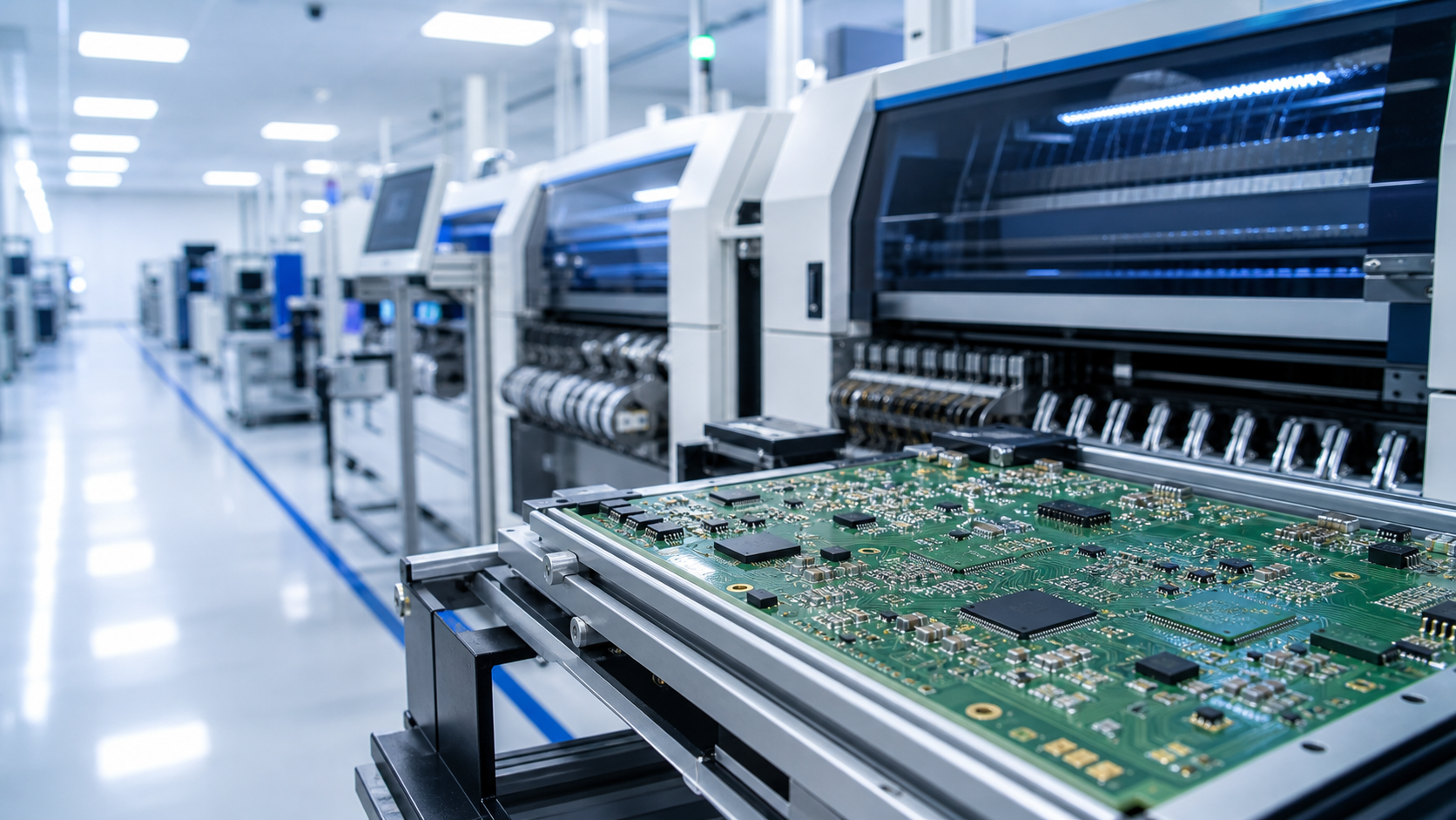
Pick-and-place equipment retrieves components from feeders, verifies their orientation and places them on the printed solder deposits. A single assembly may combine small resistors and capacitors with larger ICs, connectors and power devices, so placement programs must account for package type, nozzle selection, rotation and placement force.
Consistent placement depends on more than machine speed. Key controls include:
- Correct feeder setup and material verification
- Component polarity and orientation checks
- Barcode or lot traceability where required
- Placement accuracy for fine-pitch packages
- Controlled handling of moisture-sensitive components
- First-article verification before the full run
Modern equipment can place components at high speed, but stable results come from disciplined setup and verification.
4. Reflow Soldering and Thermal Profile Control
After placement, the assembly travels through a reflow oven. Its thermal profile normally includes preheat, soak, reflow and cooling stages. The objective is to activate the flux, bring the board and components to the required temperature, form reliable solder joints and cool the assembly without creating unnecessary thermal stress.
The correct profile depends on board thickness, copper distribution, component mass, solder alloy and package sensitivity. A profile that works for a small control board may not suit a dense power assembly with large thermal masses.
Poor thermal control can contribute to defects such as incomplete wetting, voiding, tombstoning, bridging or component damage. For this reason, profiles should be developed and verified for the assembly rather than treated as a universal machine setting.
5. AOI, X-Ray and Visual Inspection
Automated optical inspection uses cameras and controlled lighting to compare the assembled board with defined criteria. AOI can help identify missing or shifted components, polarity errors, lifted leads, solder bridges and other visible defects.
Not every joint is visible. Ball grid arrays and other bottom-terminated components may require X-ray inspection when the design, risk level or customer specification calls for it. X-ray can reveal hidden alignment issues, opens, bridges or excessive voiding that optical systems cannot see.
Manual visual inspection remains useful for confirming unusual findings and checking areas that automated systems may not evaluate well. The most effective inspection plan combines the methods appropriate to the product rather than relying on a single tool.
6. Through-Hole Assembly and Soldering
Many industrial controllers, motor drives and power products include connectors, transformers, relays or other through-hole components. These parts may be inserted manually or with automated equipment, then soldered using wave, selective or manual soldering processes.
The best method depends on component mix, board design, thermal requirements and production volume. Process controls should address lead length, component seating, solder fill, heat exposure and protection of nearby surface-mount parts.
7. Cleaning and Conformal Coating
Cleaning requirements depend on the soldering materials, product environment and customer specification. When cleaning is required, the process should remove relevant residues without trapping contamination under components or damaging labels and materials.
Assemblies intended for humid, dusty or chemically challenging environments may also use conformal coating. The coating type, thickness, masking areas, cure process and inspection criteria must be defined for the application. Conformal coating can improve environmental protection, but it does not correct poor board layout, contamination or defective solder joints.
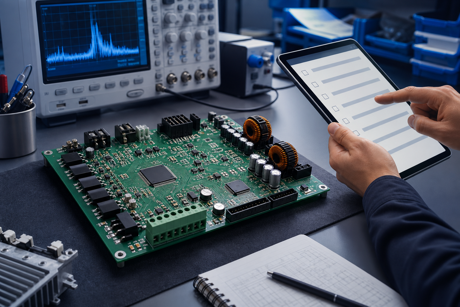
8. ICT, Programming and Functional Testing
Inspection answers whether the assembly appears to have been built correctly. Electrical testing answers whether it behaves correctly.
In-circuit testing can check selected component values, connectivity, opens and shorts through accessible test points. Programming stations load firmware or configuration data. Functional testing then powers the assembly and verifies product-specific behaviour such as voltage rails, communication interfaces, sensors, outputs, motor-control functions or protection logic.
The exact test strategy should be developed with the product architecture and risk in mind. High-reliability or safety-related products may also need boundary scan, burn-in, environmental tests or customer-defined validation procedures.
9. Final Inspection, Traceability and Production Release
Before shipment, the manufacturer confirms the required records and release criteria. Depending on the project, this may include:
- Inspection and electrical-test results
- Firmware and hardware revision records
- Serial numbers or production-lot data
- Approved deviation and rework records
- Packaging and ESD controls
- First-article or sample approval documentation
Traceability helps isolate issues, manage revisions and support future production. It is especially valuable when a project uses controlled components, multiple firmware versions or certification-related materials.
What to Ask a PCBA Manufacturing Partner
Equipment lists alone do not demonstrate manufacturing capability. When evaluating a partner, ask how the company manages the complete production system:
- How are DFM and DFT issues reviewed before release?
- How are BOM changes and component substitutions approved?
- Which inspection methods are used, and when is X-ray available?
- Can the team develop fixtures and functional-test procedures?
- How are first articles, nonconformities and rework controlled?
- What material, lot and revision traceability can be provided?
- How are prototype findings transferred into repeat production?
Clear answers to these questions are more useful than a generic promise of “high quality.”
From Design Files to a Tested PCBA
The strongest PCBA programs connect design, sourcing, manufacturing and testing from the beginning. That connection helps teams find risk earlier, reduce avoidable redesign and move from prototype builds to repeatable production with better control.
MaxMait Electronics supports custom electronic product development from schematic and PCB layout through embedded firmware, prototyping, testing and customized manufacturing. Explore our custom electronic solutions and product development capabilities, or send us your project requirements for an engineering review.
If your product is intended for the United States or Canada, you may also find our guide to FCC planning and UL-recognized materials for custom PCBA projects useful.
Frequently Asked Questions
What is the difference between a PCB and a PCBA?
A PCB is the fabricated printed circuit board before electronic components are assembled. A PCBA is the completed assembly after components have been placed and soldered, although programming, testing and final integration may still be required.
What are the main stages of PCBA manufacturing?
Typical stages include engineering review, solder paste printing, SMT placement, reflow soldering, inspection, through-hole assembly where needed, cleaning or coating, programming, electrical testing and final quality release. The exact process depends on the design and product requirements.
Are AOI and functional testing the same?
No. AOI checks visible assembly features such as component presence, position and solder-joint appearance. Functional testing powers the assembly and verifies that it performs the required product functions. Both can be important because a board may look correct but still have an electrical or firmware-related fault.
When is X-ray inspection used in PCB assembly?
X-ray inspection is commonly considered for hidden solder joints, including BGA and other bottom-terminated packages, or when the product’s risk and acceptance criteria require additional verification.